








LG Innotek is showcasing its semiconductor substrate technologies at the 2026 Electronic Components and Technology Conference (ECTC) in Orlando, Florida. The event runs from May 26 to 29 and is hosted by the IEEE. ECTC is the world's premier international event for semiconductor packaging, drawing over 2,000 attendees and 135 leading firms, including Intel, Amkor, ASE, and IBM.
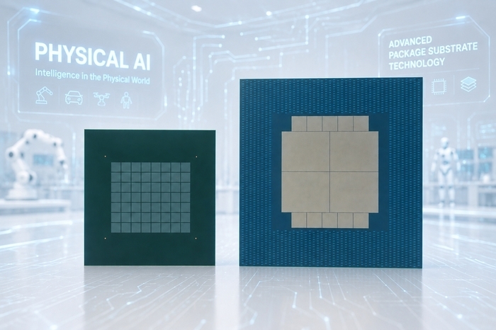
At its dedicated exhibition booth, LG Innotek unveiled a large-format Flip Chip Ball Grid Array (FC-BGA) substrate measuring 85mm x 85mm, alongside a prototype of an even larger substrate, with a surface area nearly 40% greater. As AI semiconductors become increasingly sophisticated, these substrates are evolving to accommodate more circuits and components through higher layer counts, increased density, and expanded dimensions.
A key highlight of the large-format FC-BGA is the integration of “Chip Embedding” technology. Unlike traditional methods where chips are mounted on top of the substrate, LG Innotek's approach embeds the chip directly inside the substrate. This significantly shortens signal paths and reduces electrical resistance during power delivery by approximately 25%, lowering server power loss and improving energy efficiency.
The company also featured its Radio Frequency System-in-Package (RF-SiP) substrates for 5G communications. Currently in mass production using the “Copper Post” method, these substrates offer higher circuit density and are 20% thinner than conventional designs. This enables the development of high-performance, ultra-slim smartphones.
“ECTC serves as a vital platform for LG Innotek to showcase its competitive edge in next-generation substrate technology and to expand strategic partnerships with global customers,” said Jitae Cho, Head of the Package Solution Business Unit at LG Innotek. “We aim to grow the package solution business into a core business, targeting revenues exceeding 3 trillion KRW by 2030.”
