








Intel is ramping up its foundry resurgence by committing to a large-scale expansion of its advanced semiconductor packaging capabilities. By securing a robust infrastructure of materials, components, and equipment, the tech giant aims to significantly boost its production capacity to meet the demands of its newly won foundry clients.
Industry sources reported on May 28 that Intel is currently issuing large-scale purchase orders to global supply chain partners. Multiple contracts for materials and equipment have reportedly been finalized, with several South Korean firms among the participants.
“A multi-trillion won (multi-billion dollar) investment in advanced packaging facilities is underway,” an industry insider familiar with the matter stated. “Given the lead times for equipment and materials, full-scale operation is expected by next year.” Discussions for further investments through 2028 are also reportedly in progress, with production hubs in the U.S., Vietnam, and Malaysia cited as primary locations.
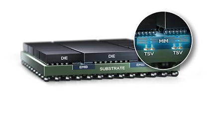
The core of this investment focuses on expanding the capacity of Intel's proprietary EMIB (Embedded Multi-die Interconnect Bridge) technology.
EMIB is a 2.5D packaging solution that connects different semiconductor dies using a silicon bridge embedded within the substrate. Compared to the silicon interposer-based 2.5D packaging pioneered by TSMC, EMIB is widely seen as offering superior cost-efficiency and manufacturing productivity. The key advantage is that bridges can be applied only where needed, enabling highly tailored 2.5D integration.
Intel is further advancing this ecosystem with “EMIB-T,” which incorporates Through-Silicon Via (TSV) technology into the bridge, and next-generation solutions utilizing glass substrates. These innovations aim to diversify Intel's packaging portfolio and broaden its customer base. A significant portion of the current equipment investment is dedicated to these next-generation technologies.
This aggressive move into packaging is a strategic cornerstone for Intel's broader foundry ambitions. Since announcing its re-entry into the foundry business in 2021, Intel has faced challenges in securing high-profile clients, as TSMC continues to dominate the production of advanced AI chips.
By prioritizing packaging, Intel is leveraging a differentiated capability to attract customers. As the industry hits the physical limits of circuit miniaturization in front-end processes (wafer fabrication), advanced packaging (back-end) has emerged as the new frontier for boosting chip performance. Intel's strategy is to overcome these technical hurdles through back-end innovation, thereby stabilizing its entire foundry business.
The company is maximizing synergy by advancing its front-end processes simultaneously. Last year, Intel operationalized its 1.8nm-class Intel 18A process and has continued investing in facilities to serve both its own internal chips and external foundry clients.
“This massive investment in packaging is a clear signal that Intel has secured a meaningful pipeline of advanced process customers,” another industry expert noted. “The expansion of both the 18A process and advanced packaging marks the true beginning of Intel's foundry comeback.”
