


Taiwan Semiconductor Manufacturing Co. (TSMC) is heading for a high-stakes showdown with Samsung Electronics over next-generation semiconductor packaging technology.
As TSMC accelerates plans to commercialize Panel-Level Packaging (PLP) -- a technology that significantly improves productivity for artificial intelligence (AI) chips -- a fierce battle for market leadership with industry pioneer Samsung Electronics appears inevitable.
According to semiconductor industry sources, TSMC is actively building both local and global supply chains for materials, components and equipment to establish a robust PLP mass-production ecosystem. The Taiwanese foundry giant is in advanced talks with multiple equipment suppliers and is aiming to begin volume production as early as next year.
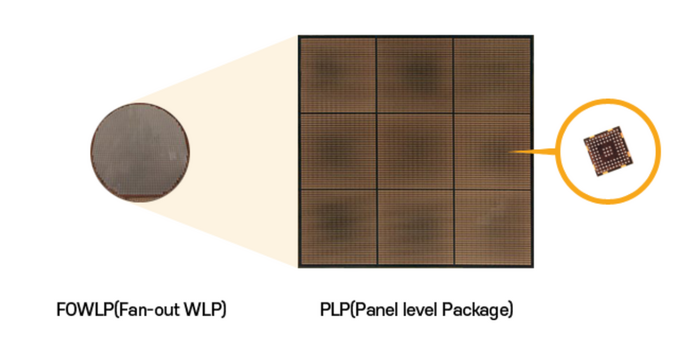
PLP is an advanced packaging method in which diced silicon chips (dies) are rearranged and packaged on a large rectangular panel instead of a traditional circular wafer, contrasting with conventional Wafer-Level Packaging (WLP). When packaging on a round wafer, the curved edges leave unusable areas, resulting in material waste and lower yields. Moving to rectangular panels eliminates these dead zones. A standard 600×600 mm panel can typically yield five to six times more chips than a mainstream 300 mm (12-inch) circular wafer.
Samsung Electronics currently holds the upper hand in PLP. After acquiring the PLP business from Samsung Electro-Mechanics in 2019, the company has built deep expertise by applying the technology to mobile application processors (APs) and power management integrated circuits (PMICs).
TSMC, by contrast, had long taken a cautious stance toward PLP, relying instead on its dominant position in wafer-level packaging to support its foundry leadership. But the explosive growth of AI has shifted the market paradigm. PLP has rapidly emerged as a critical technology because it not only scales up production volume but also offers a distinct advantage for manufacturing ultra-large-die AI chips that combine multiple components such as HBM.
In response, TSMC launched its PLP roadmap in 2024. After bringing a pilot line online this year, the company is expected to move to high-volume manufacturing next year, following final performance evaluations. Industry reports suggest TSMC has already secured commitments from major global AI chip customers.
As TSMC accelerates its schedule, competition with Samsung is set to intensify. Samsung is expanding its PLP applications beyond mobile APs and PMICs to high-performance computing (HPC) devices, including advanced AI processors. Glass substrates -- widely touted as the future of AI chip packaging -- are also expected to be integrated into this PLP workflow, creating yet another battleground between the two rivals.
“The race isn't limited to just Samsung and TSMC,” an industry insider said. “Major global outsourced semiconductor assembly and test (OSAT) players are also moving aggressively into PLP. The market is poised for exponential growth driven by intense competition.”
