








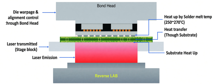
Semiconductor packaging and test company Amkor Technology has put its large-package bonding process, R-LTC, front and center in the U.S. market. Developed at Amkor's research center in Korea, R-LTC is a bonding technology that reduces defects in large-substrate AI packages. The move appears aimed at winning more U.S. customers ahead of the company's Arizona plant, which is scheduled to begin operating in 2028.
According to industry sources on Thursday, Amkor presented a paper at the International Microelectronics Assembly and Packaging Society (IMAPS) annual symposium, held from Sep. 28 to Oct. 1 local time. The paper was titled “Reducing Thermal Stress and Warpage in Chiplet Modules with Reverse Laser-assisted Thermocompression Bonding (R-LTC).”
The core of the presentation was a proposed answer to two questions: what structure large packages should use, and how to attach such a large body to the substrate. The bigger and higher-performance the package substrate, the worse thermal, electrical signal, power delivery, warpage and design challenges become, all at once.
R-LTC targets warpage, which arises as AI accelerator substrates grow larger. Silicon and the substrate expand differently when heated, and that mismatch bends the package. According to Amkor's research, warpage on a roughly 3-reticle module (54 x 46 mm, with two ASICs and eight high-bandwidth memory (HBM) stacks) is more than three times worse than on a roughly 1-reticle module (33 x 26 mm). That suggests advanced packaging technologies that reduce warpage and stress will only become more important.
The technology builds on Amkor's laser-assisted bonding (LAB), which the company introduced in 2014. In 2021, it evolved to fire the laser from beneath the substrate instead of from above, because a laser from above is blocked by plastic mold or a metal backside. R-LTC, which followed, keeps the laser heating from below and adds thermocompression bonding (TCB), which presses the die down from above at the same time.
The process is aimed at products with large bodies, such as data center CPUs, 2.5D packages and high-density fan-out packages. This year, Amkor signed a multiyear, prepayment-backed packaging agreement with Nvidia worth $1.5 billion, as well as a 10-year agreement with TSMC (terms undisclosed). Both deals secure capacity before Amkor's Arizona plant comes online.
Amkor has said on several occasions that it plans to mass-produce products in Korea first and then move them to Arizona, including at its Investor Day in May and at an Arizona economic delegation event in August. At a Goldman Sachs conference this month, it described Nvidia's $1.5 billion prepayment as an “anchor customer” that enables the transfer of technology from Korea to Arizona.
Amkor's U.S. plant sits close to TSMC's Arizona fab, so further collaboration on multiple fronts is expected. The company's planned local investment has climbed steadily, from about $2 billion in 2023 to $7 billion in 2025 and about $12 billion as of September 2026. After customer volumes already exceeded the first-phase cleanroom of about 33,000 square meters, Amkor added a 60,000-square-meter second phase, bringing the total to about 93,000 square meters. The two phases combined are expected to create more than 3,500 jobs.
