








Plan delivered to members of Council of Cooperative Companies
Sharing of semiconductor process data to be expanded
Solving technological challenges and advancing product sophistication
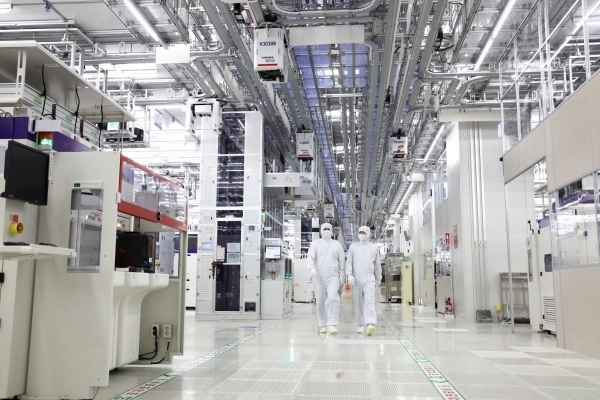
Samsung Electronics Co., Ltd. will expand its pattern wafer support for domestic small and medium-sized enterprises (SMEs) and middle-market companies to strengthen the semiconductor materials, parts, and equipment (materials/parts/equipment) cooperation ecosystem. This means sharing more semiconductor process data with cooperative partners over a broader range of areas, which is expected to provide an opportunity to solve technological challenges that the materials/parts/equipment industry has not been able to resolve until now, and to further elevate their technological capabilities.
According to the industry on July 9, Samsung Electronics plans to expand the volume and scope of pattern wafer support for materials/parts/equipment companies cooperating with its Device Solutions (DS) Division. It has been confirmed that Song Jae-hyuk, president and chief technology officer (CTO) of the Samsung Electronics DS Division, recently shared this information with materials/parts/equipment companies belonging to the Samsung Electronics Council of Cooperative Companies (Hyubsung-hoe).
A CEO of a materials/parts/equipment company who is knowledgeable about the matter stated, “Samsung Electronics conveyed a policy to strengthen pattern wafer support in order to grow together with its materials/parts/equipment cooperative partners,” and added, “The plan is to increase the volume of pattern wafers provided and expand the scope of processes, which had been limited until now due to security issues.”
A pattern wafer, which means a wafer with circuits drawn on it, is an essential element for the technological sophistication of materials/parts/equipment. This is because it is a physical means to identify whether various materials and equipment work properly in an actual semiconductor manufacturing line and whether there are any process defects. Only after looking at the results of the pattern wafer can data be secured to improve and upgrade materials and equipment.
Currently, pattern wafer support is organized by the Korea Semiconductor Industry Association (KSIA). When materials/parts/equipment companies make a request, bare wafers (pre-processing stage) are secured as much as the required volume, and the request is made to semiconductor manufacturers such as Samsung Electronics. When Samsung Electronics fabricates the pattern wafers, the materials/parts/equipment companies receive them back and utilize them for product development and improvement.

Samsung Electronics has been providing about 1,000 pattern wafers annually to its materials/parts/equipment cooperative partners. However, as the number of process steps has expanded from hundreds to thousands, the demand for pattern wafers required by cooperative partners has surged.
An industry official evaluated, “Although the necessity for pattern wafers has grown, from the perspective of semiconductor manufacturers, it can be a burden to expand supply because process information goes outside,” and added, “The fact that a semiconductor manufacturer is taking the lead in expanding supply is a very forward-looking measure.”
The industry expected that Samsung Electronics' expansion of pattern wafers will serve as an opportunity to solve technological challenges in materials/parts/equipment and advance product sophistication.
It is observed that Samsung Electronics will discuss expanding the volume of provision in consideration of requests from cooperative partners in the future. In addition, it is known that the company will maximize the effect of pattern wafer support by sharing not only pattern wafers from specific processes but also the results of pre- and post-processes with cooperative partners.
Samsung Electronics' unconventional move is interpreted as a judgment that continuous growth is difficult unless the materials/parts/equipment ecosystem surrounding semiconductor manufacturing is solid. It means that only when the technological strength of cooperating materials/parts/equipment is pulled up can the semiconductor manufacturing capability of Samsung Electronics be strengthened together. This is in the same context as recent moves by the United States, China, and Japan to support their materials/parts/equipment ecosystems and induce technological sophistication.
Previously, Samsung Electronics decided to expand the companies participating in 'DSEP', a process data sharing ecosystem platform. DSEP is being operated with the purpose of sharing information related to Samsung Electronics semiconductor manufacturing with cooperative partners, thereby sophisticatedly upgrading equipment and increasing productivity.
