




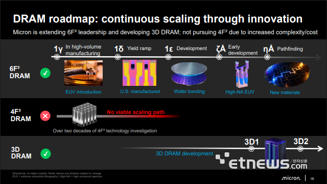
U.S. memory chipmaker Micron Technology has officially abandoned plans to adopt the 4F² (4F-square) cell architecture, considered a critical milestone in next-generation DRAM scaling. Instead of pushing ahead with 4F², Micron has decided to extend the existing 6F² architecture and focus on a technology roadmap centered on wafer bonding and three-dimensional (3D) stacking. The move is seen as a strategic bet to reverse its competitive position against South Korean rivals.
Micron announced the decision during a technology webinar held on Oct. 21 (local time), where it unveiled a multigenerational technology roadmap outlining its memory development strategy for the next decade. The most significant revelation during the presentation was Micron's assessment of next-generation DRAM architectures.
Samsung Electronics and SK hynix are currently researching a 4F² architecture based on vertical channel transistors (VCTs) to overcome the physical limitations of sub-10-nanometer (0a- and 0b-class) manufacturing processes. Their strategy is to reduce the existing 6F² cell structure to 4F², shrinking chip area and increasing integration density.
In its presentation materials, Micron explicitly stated that it had researched 4F² for more than 20 years but found “no viable scaling path.” Scott DeBoer, president and chief technology and product officer (CTPO) of Micron, who delivered the presentation, said there were “fundamental problems” with 4F² scaling and described its density advantage over 6F² as “somewhat of a myth.”
Rather than pursuing 4F², Micron has placed wafer bonding and 3D DRAM at the forefront of its roadmap. Following its current mainstream 1-gamma (1γ) technology, the company plans to begin mass production of next-generation 1-delta (1δ) DRAM in Boise, Idaho, in the second half of 2027. It will then introduce wafer bonding technology on a full scale in 1-epsilon (1ε), a subsequent node based on the 6F² architecture that is reportedly progressing smoothly through development.
In particular, Micron has officially positioned 3D DRAM technologies, designated 3D1 and 3D2, between the 1-zeta (1ζ) and 1-eta (1η) nodes in the advanced stages of its roadmap. The strategy is to pursue high-numerical-aperture extreme ultraviolet (High-NA EUV) lithography equipment and explore new materials while preparing to introduce 3D DRAM into commercial production lines as soon as it becomes economically viable.
In packaging and high-bandwidth memory (HBM), Micron also unveiled a new concept called Vertical HBM, which maximizes the use of 3D stacking technology. While conventional HBM is positioned alongside a processor (XPU) on an interposer, Vertical HBM places memory directly on top of the processor and connects the two using fine-pitch hybrid bonding.
Industry observers view the announcement as a bold strategic move by Micron to reshape its technological competition with Samsung Electronics and SK hynix. Rather than competing directly over 4F², long considered the final steppingstone in two-dimensional scaling, Micron is signaling its intention to change the rules of competition first through bonding and 3D stacking technologies.
Meanwhile, Chinese memory chipmaker ChangXin Memory Technologies (CXMT) recently announced plans to commercialize server DRAM based on a 4F² architecture, triggering volatility in memory semiconductor stocks worldwide. Shares of South Korean companies, including Samsung Electronics and SK hynix, also fell sharply, underscoring the market's sensitivity to technological competition.
