




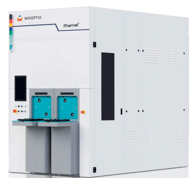
Wooptix, a Spanish metrology equipment startup backed by investors including Samsung, Intel and Tokyo Electron (TEL), has brought its equipment into a South Korean semiconductor company and begun initial collaboration. The move is expected to challenge the dominance of U.S.-based KLA in the semiconductor wafer shape and stress metrology market.
According to industry sources on Oct. 20, Wooptix recently installed a laboratory system at a South Korean semiconductor company and began technology verification and collaboration. Although the partner company and scope of cooperation have not been disclosed, attention is focused on whether Samsung Electronics will eventually introduce the equipment into its main production processes, given Samsung's equity investment in Wooptix.
Wooptix is reportedly considering entering advanced foundry processes first before expanding applications into the memory sector.
Wooptix develops equipment that uses wavefront phase imaging (WFPI) technology to measure the shape, warpage, nanotopography and stress of an entire wafer in a single measurement. With higher measurement speeds and resolution than conventional methods, the technology is attracting attention as a potential game changer in wafer shape control, a critical factor affecting yields in advanced semiconductor manufacturing and advanced packaging.
Until now, U.S.-based KLA has dominated the semiconductor defect inspection and metrology equipment market with an overwhelming market share. KLA's equipment offers advantages in reliability proven over years of use in mass-production lines, comprehensive metrology capabilities that include simultaneous measurements of both wafer surfaces and thickness information, and integration with factory process control systems.
By comparison, Wooptix's WFPI technology can measure the shape of an entire wafer in a single shot and is less sensitive to vibration. It can also perform measurements on wafers that have undergone intermediate processing steps involving patterns or oxide films. The company emphasizes the technology's distinctive speed and precision. For South Korea's semiconductor industry, this opens up an opportunity to diversify its supply chain beyond KLA in a critical area of metrology.
Wooptix's equipment is expected to demonstrate its greatest value in advanced packaging processes, including high-bandwidth memory (HBM), die-to-wafer (D2W) and wafer-to-wafer (W2W) bonding. This is because the equipment can precisely detect microscopic gaps known as voids, lifting or separation that occurs during chip stacking, die flatness and the degree of wafer warpage after bonding. Although the technology is also used to check interlayer alignment in advanced logic foundry processes, it is currently considered more useful in packaging applications.
Accordingly, Samsung Electronics, which operates both foundry and HBM businesses, and SK hynix, a leader in the HBM market, are considered the most likely initial partners in South Korea.
Wooptix is also accelerating its global market expansion. After installing its first fully automated system in the cleanroom of French research institute CEA-Leti in June, the company plans to begin joint development with global semiconductor manufacturers next year and expand equipment supplies to mass-production lines.
“South Korea is a very important market for us because it is home to Samsung and SK hynix,” a Wooptix official said. “We are keeping new possibilities open for high-volume manufacturing (HVM) and will significantly strengthen our activities in the Korean market.”
