








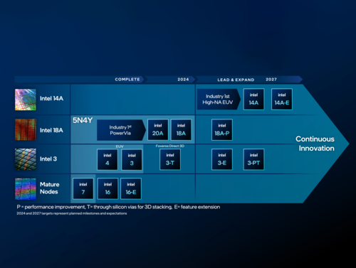
Intel is internally considering a dual-side power delivery architecture--utilizing both the front and back of the wafer--for its 1.4-nanometer-class process as it seeks to close the gap with foundry rivals.
According to industry sources, Intel originally planned to implement “PowerDirect”--its proprietary backside power delivery network (BSPDN) technology--for its baseline 1.4nm process, known as 14A. However, for the subsequent 14A2 node, the chipmaker is now evaluating a hybrid “dual-side” architecture that taps both frontside and backside routing.
This structural pivot is directly tied to lithography limitations--specifically stochastic defects--that arise as Intel pushes its tightest metal layer, the minimum metal pitch (M0), down to the 21nm range.
To outpace TSMC's N2/A14 and Samsung's SF2Z nodes, Intel has previously announced plans to boost chip density by about 1.3× compared with its 18A node. While the target M0 pitch for the 14A node is around 28nm, analysts believe Intel will aggressively push the M0 pitch to 21nm in the 14A2 node through a half-node scaling approach. At 21nm, even with the need for double patterning, the resulting density gains would improve the economic viability of High-NA EUV lithography systems, which cost hundreds of millions of dollars per unit.
The critical hurdle, however, is that wiring resistance rises sharply when circuit lines shrink below roughly 21nm. The nano-through-silicon-via (nTSV) infrastructure, originally built solely for backside power delivery, cannot handle the extreme current density required by the transistors. This triggers severe voltage drops, a phenomenon known as IR drop.
Consequently, analysts suggest Intel is opting for a hybrid structure: keeping the BSPDN as the primary power network while re-allocating a portion of the frontside metal layers to auxiliary power and clock signaling. This is intended to regain power margins lost to aggressive scaling and lithography limits. Experts view this as a strategic compromise; despite the downside of increased routing complexity, Intel is modifying its architecture to push the demanding 21nm process specifications.
Intel also faces intense time pressure. According to its roadmap, the 14A node is scheduled for risk production in 2028, with high-volume manufacturing slated for 2029. Under this tight schedule, Intel plans to release version 0.9 of its process design kit (PDK) for the 14A node to external customers this October. The company faces a high-stakes challenge to secure firm orders from major fabless clients within the next 18 months.
Meanwhile, its competitors are moving quickly. TSMC has already secured stable yields for its 2nm (N2) node across 2025 and 2026, entering the market in tandem with product launches from its anchor customer, Apple. Furthermore, by 2028--when Intel expects to begin 14A risk production--TSMC plans to be shipping finished 1.4nm (A14) products to the market. Samsung Electronics is also on track to commercialize SF2Z, its enhanced 2nm process featuring backside power delivery, by 2027. Samsung's biggest leverage is its operational maturity with gate-all-around (GAA) transistors, a technology it has been refining since its 3nm node.
An industry insider noted, “While Intel is struggling with yield ramp-ups because it is introducing GAA and BSPDN simultaneously at the 20A/18A nodes, Samsung faces significantly lower technical risk. Samsung is simply overlaying backside power delivery onto a 2nm GAA structure that has already been thoroughly vetted.”
