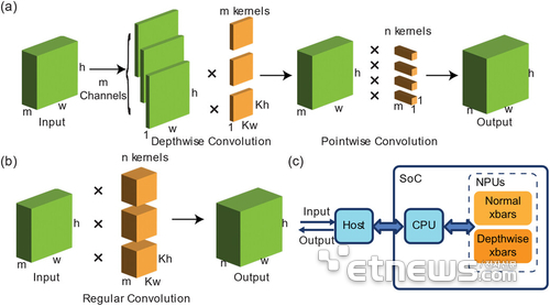







SK Hynix, in collaboration with U.S. semiconductor startup Tetramem, has successfully validated a next-generation artificial intelligence (AI) chip technology that performs data processing directly within memory. The newly developed memristor-based In-Memory Computing (IMC) System-on-Chip (SoC) is drawing significant industry attention as a breakthrough that could substantially improve AI power efficiency in the post-HBM era.
According to both companies, their joint paper, titled “A Memristor-Based In-Memory Computing SoC with Efficient Depthwise Convolution,” was recently published in the international journal Advanced Intelligent Systems. The study details the physical implementation of a memory-device-based computing architecture into an actual SoC, confirming its high performance and efficiency during AI inference tasks.
In-Memory Computing represents a paradigm shift by executing calculations where data resides, in contrast to traditional architectures that must constantly shuttle data between memory and a processor. As AI models grow exponentially in scale, this conventional data movement creates severe power bottlenecks and processing delays. IMC is widely considered a leading next-generation approach to eliminating these bottlenecks. While HBM addresses the issue by vertically stacking DRAM to widen the data highway to the processor, IMC instead minimizes the need for data movement altogether.
The core breakthrough of this joint research lies in the hardware validation of “depthwise convolution” -- an operation notoriously difficult to implement efficiently in existing IMC setups. Depthwise convolution is a key technique used in lightweight, mobile-friendly AI models to reduce computational workloads.
According to the paper, the validated SoC was fabricated using a 65nm CMOS process and achieved an energy efficiency of 21.3 TOPS/W at a 100MHz operating frequency. Running a customized MobileNetV1 model tuned for the Visual Wake Words (VWW) dataset, the chip achieved an inference accuracy of 80.36% -- comparable to equivalent software models quantized to 4-bit precision, supporting its real-world viability.
In this project, SK Hynix contributed its expertise in memory devices, fabrication processes, and back-end packaging technologies to physically realize the chip, while Tetramem led the circuit design and computing architecture. Founded in 2018 and based in California, Tetramem is a specialized startup developing analog-memory-based computing platforms, with a focus on improving AI processing efficiency through next-generation memory devices such as memristors.
“This project demonstrates the value of exploring innovative memory technologies and new computing architectures for future AI systems,” said Kim Soo-gil, Vice President at SK Hynix. “We look forward to continued technological exchange with the Tetramem team in areas of mutual interest.”