




The United States is accelerating its return as a semiconductor manufacturing powerhouse, moving beyond high-profile investment pledges toward concrete timelines for fab capacity expansion.
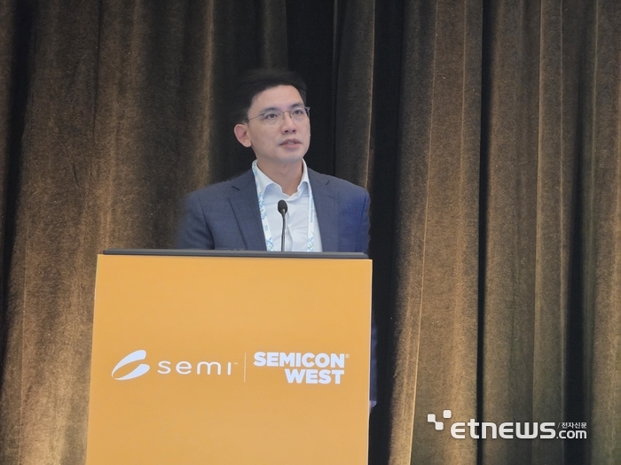
Speaking at a media briefing during SEMICON West 2026 in San Francisco on Oct. 12 (local time), Clark Tseng, Senior Director of Market Intelligence at SEMI, projected that U.S. 300mm (12-inch) fab equipment spending will more than double, surging from $18.1 billion in 2026 to $40.6 billion by 2029.
Over the same period, global 300mm fab equipment spending is forecast to expand from approximately $149 billion in 2026 to $227 billion in 2029, indicating that the pace of growth in the U.S. will significantly outstrip the global average.
Fab equipment spending on 300mm wafers covers critical capital machinery—such as lithography, etch, and deposition tools—for current-generation leading-edge logic, DRAM, and NAND flash semiconductors. A rise in these figures signals that ground is being broken for new fabs and production tooling is actively moving into existing facilities. Globally, 20 new 300mm fabs or line expansions are slated to break ground in 2026, followed by 18 in 2027, with the U.S. accounting for three and four of these projects, respectively.
Milestones for “first silicon”—marking the operational startup of new facilities—are expected to climb globally from 13 fabs in 2026 to 23 in 2027. Key marquee projects include advanced logic and foundry investments by Intel, TSMC, and Samsung Electronics, DRAM expansions by Micron Technology, and analog capacity buildouts by Texas Instruments (TI). SEMI assessed that, despite this massive infrastructure buildout, the industry faces little risk of structural overcapacity.
“All chipmakers are closely reviewing their internal forecasts, and the industry stands ready to flexibly adjust its plans should any signs of a market slowdown or correction emerge,” Tseng explained. “At present, however, producers are racing simply to keep pace with demand.”
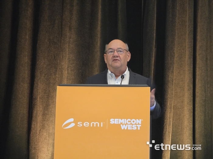
This expanding manufacturing footprint is also driving unprecedented demand for industry exhibitions and technical conferences. Joe Stockunas, President of SEMI Americas, noted, “Exhibition booths at this year's SEMICON West are completely sold out, with a waitlist of 120 companies we simply couldn't accommodate.” He added, “Attendance is already pacing ahead of last year, and we anticipate drawing up to 40,000 visitors throughout this week's event,” eclipsing the previous record of 37,000 set in Phoenix last year.
As North America's premier semiconductor conference, SEMICON West has called the San Francisco Bay Area its home for over five decades, reflecting the region's historic role as the cradle and epicenter of the global chip industry since its rapid ascent in the 1970s.
Beginning next year, however, SEMI will relocate the flagship event to Phoenix, Arizona—a strategic move mirroring the broader geographic shift of the U.S. semiconductor manufacturing hub toward the Desert Southwest.
To date, cumulative semiconductor-related investments across the United States have reached $828 billion, with $319 billion concentrated in Arizona alone, anchored by Phoenix. TSMC's standalone commitment to its Arizona fab complex accounts for $265 billion of that total. These regional projects are slated to generate 60,000 direct semiconductor jobs, alongside an estimated 180,000 indirect jobs across the surrounding supply ecosystem.
“The U.S. CHIPS and Science Act has served as a powerful catalyst,” Stockunas emphasized. “The rapid expansion of domestic manufacturing capacity is directly driving demand across our exhibition floors and technical sessions.”
