








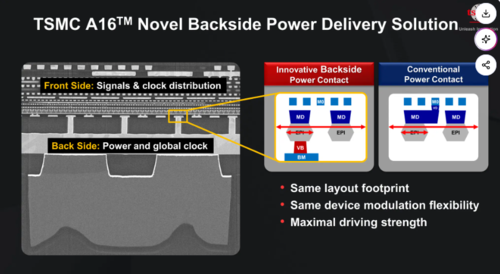
TSMC has taken an early lead in angstrom-class semiconductor manufacturing by securing an advantage in backside power delivery for its A16 process, an advanced node below 2 nanometers. The technology is designed to address bottlenecks caused by power and signal routing competing for the same space on the front side of conventional chips.
According to industry sources on the 18th, TSMC has successfully developed and validated A16, the industry's first angstrom-class CMOS platform to incorporate its Super Power Rail (SPR) backside power-delivery architecture. The key achievement is that A16 preserves the gate density and NanoFlex design flexibility of the N2P process, an enhanced version of TSMC's N2 node.
In conventional semiconductor chips, both power interconnects and signal interconnects are placed on the front side of the die. As process nodes shrink, the two increasingly compete for limited routing space, leading to more severe wiring congestion and higher resistance-related voltage drops, commonly known as IR drop.
Implementing backside power delivery has typically required substantial changes to transistor placement and standard-cell structures. At more advanced nodes, supplying power through the back of the chip often means sacrificing portions of existing cell libraries and design methodologies.
TSMC separates the power-delivery network entirely onto the backside of the die and uses dedicated vertical back-side contacts, or VBs, to connect power directly to the source and drain regions of each transistor. The company achieved this while making minimal changes to the front-side gate structure, cell dimensions and layout footprint, preserving compatibility with established chip designs.
The performance gains are also substantial. Compared with N2P, A16 can deliver 8% to 10% higher speed at the same power level, or reduce power consumption by 15% to 20% at the same speed. Chip density can also improve by 8% to 10%.
The process is considered particularly well suited for AI and high-performance computing chips, which require complex signal routing and dense power networks. Mass production of the A16 process is scheduled to begin in the fourth quarter of this year.
Intel, which commercialized backside power delivery earlier with its PowerVia technology, had to modify its existing cell architecture during testing, including adjustments to pin counts and relaxed metal pitches. Samsung Electronics is also reported to be pursuing backside power delivery for its SF2 process, likely through an approach similar to Intel's.
“This achievement can improve efficiency while reducing design burden for products such as AI accelerators, which must secure both power efficiency and performance,” an industry source said. “In the angstrom era, competition is intensifying not only in process technology but also across the design ecosystem.”
