








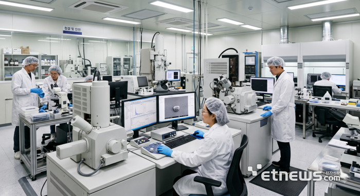
Samsung Electronics Co., Ltd. and SK Hynix Inc. are massively upgrading their 'analysis labs', which are core infrastructure for semiconductor process improvement and yield management. They plan to introduce next-generation inspection and analysis equipment to build up their capabilities to secure advanced semiconductor yields.
According to the industry on Aug. 18, the DS division of Samsung Electronics began upgrading its semiconductor process analysis labs. It was confirmed that the company is promoting the introduction of next-generation equipment through partners to inspect semiconductor and wafer circuit patterns or diagnose defects.
An industry official familiar with the matter explained, “Beyond conducting process analysis on a traditional semiconductor chip (die) basis, we are preparing new infrastructure that can inspect and understand the wafer itself,” adding, “It is a move to establish next-generation semiconductor analysis labs.”
An analysis lab is diagnostic infrastructure for securing yield and reliability in semiconductor manufacturing and determining whether processes need improvement. Through various measurement and inspection equipment, it detects anomalies occurring in processes and derives why problems occur and how to solve them. Through this, process, equipment, design, and material departments share areas to be improved and support decision-making.
Samsung Electronics operates analysis labs in each business division and process line, including memory, foundry (contract manufacturing), and packaging, performing evaluation and analysis functions.
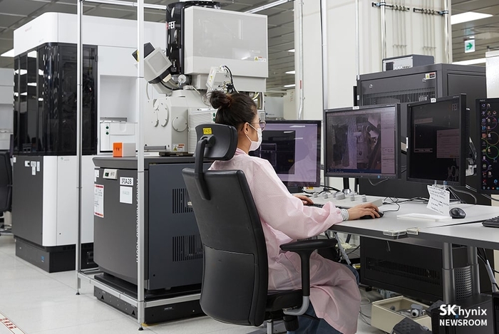
SK Hynix is also pursuing a generational transition of its analysis labs. SK Hynix integrated scattered analysis lab functions into one and is operating an 'Analysis Technology Center.' SK Hynix is also understood to be considering improvement plans to upgrade center facilities.
The moves by both companies are interpreted as a preparation to raise yields of major semiconductor products. As semiconductor circuits become finer and process difficulty increases with the application of advanced packaging, demand for analyzing defects and other issues has grown. Yields can be increased only when these are properly managed.
Yield refers to the proportion of good products among all manufactured products. Higher yields make it possible to maximize profits. In particular, the importance of high value-added products such as High Bandwidth Memory (HBM) has grown to the point where manufacturers' financial results depend on yield. As memory prices surge recently due to the expansion of artificial intelligence (AI) infrastructure investments, this is analyzed as an attempt to maximize profitability through preemptive yield improvements.
An industry official anticipated, “In the current situation where yield management has emerged as the industry's biggest task, this is a move to meet customer requirements as much as possible and respond to market expansion through analysis lab upgrades,” adding, “The yield management competition between the two companies will become even hotter.”
