








The South Korean government has joined forces with tech powerhouses Samsung Electronics and SK hynix to engineer next-generation silicon that delivers a 100-fold leap in compute performance and energy efficiency over existing architectures. By orchestrating advances across devices, memory architectures, and heterogeneous packaging, the public-private coalition seeks to dismantle critical hardware bottlenecks—namely memory walls and escalating power consumption driven by exponential artificial intelligence (AI) workloads.
On Oct. 14, the Ministry of Science and ICT (MSIT) held an inaugural ceremony in Seoul for the steering and technical committees of its flagship “K-Moonshot” semiconductor initiative. Industry leaders and researchers from Samsung Electronics, SK hynix, Jusung Engineering, the Electronics and Telecommunications Research Institute (ETRI), and the Korea Electronics Technology Institute (KETI) convened to map out long-term technology roadmaps and strategic execution milestones.
K-Moonshot is a national research and development initiative engineered to tackle high-stakes technological challenges by converging AI with foundational science and engineering. The semiconductor mission aims to pioneer a memory-centric computing paradigm and establish South Korea as a global powerhouse in AI compute throughput. The strategic pivot reflects a structural market shift as AI expands beyond cloud-based generative models into on-device and physical AI systems, placing unprecedented premiums on ultra-low-power, high-efficiency silicon.
As its benchmark target, the initiative aims to develop semiconductor architectures capable of processing 200 tokens per watt (W) by 2035. Tokens represent the fundamental units of text parsed by Large Language Models (LLMs) and serve as the standard billing metric for commercial AI services; current hardware benchmarks stand at roughly 2 tokens per watt. Through the K-Moonshot roadmap, engineers plan to drive an 8.8-fold gain in compute throughput alongside an 11.4-fold reduction in power consumption, compounding into an overall 100-fold surge in performance-per-watt efficiency.
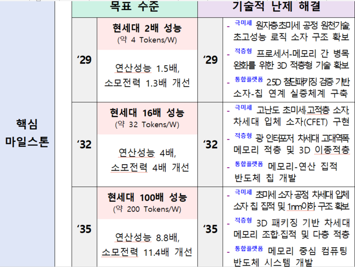
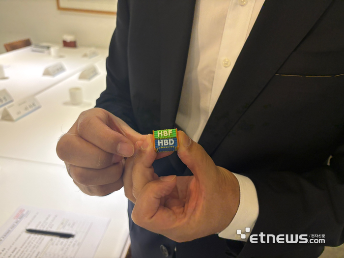
The roadmap will roll out across three designated phases: Phase 1 (2026-2029), Phase 2 (2030-2032), and Phase 3 (2033-2035), focusing sequentially on sub-nanometer nodes, vertical 3D stacking, and integrated heterogeneous platforms. A signature milestone is the development of “New HBM,” a hybrid 3D-stacked architecture that vertically integrates DRAM-based High Bandwidth DRAM (HBD) with NAND flash-based High Bandwidth Flash (HBF). While conventional High Bandwidth Memory (HBM) exclusively stacks DRAM dies optimized for raw throughput, the hybrid model incorporates high-density NAND flash to expand on-package capacity and sustain sprawling AI model parameters. MSIT has earmarked an initial budget of KRW25 billion next year to fund core R&D milestones.
In parallel, the sub-nanometer track will spearhead novel device designs and lithography process technologies for sub-1nm fabrication, while the integrated platform initiative focuses on advanced packaging breakthroughs that unite glass substrates, optical interconnects, and compute silicon into a unified system-in-package.
The K-Moonshot semiconductor program is structured around a joint validation model: academic and research institutions will spearhead foundational IP development, followed by collaborative public-private R&D projects to verify technology commercialization. Governance is divided between a steering committee tasked with strategic oversight and budget adjustments, and a technical committee responsible for roadmap execution and performance benchmarking.
Government officials emphasized that pre-emptive state backing for capital-intensive, high-risk foundational technologies—which are challenging for individual private enterprises to underwrite alone—will provide critical leverage in the intensifying global AI chip race as research is systematically funneled into frontline industrial deployment.
“In the AI era, national semiconductor supremacy will no longer hinge solely on single-chip scaling, but on our ability to interconnect device nodes, memory fabrics, and advanced packaging into a unified leap in system-wide throughput and energy efficiency,” said Kim Sung-soo, Director General of the R&D Policy Bureau at MSIT. “By mobilizing the collective expertise of industry, academia, and national research institutes, we will pre-emptively secure core foundational IP and translate laboratory breakthroughs into sustainable industrial leadership, decisively anchoring the nation's three core mega-projects.”
