




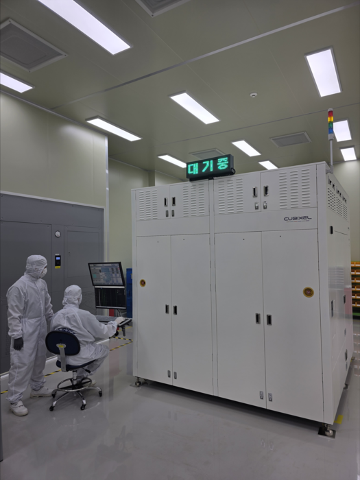
CubicCell has developed an inspection system designed to monitor through-glass vias, or TGVs, throughout the semiconductor glass-substrate manufacturing process.
The system uses the company's proprietary holography-based optical technology to inspect not only defects in completed TGV structures, but also the laser-processing, etching and final via-hole stages that determine the quality of the finished substrate. CubicCell said the technology could help improve yield and manufacturing productivity for glass substrates used in AI semiconductors.
The company said on Sept. 14 that its new equipment can detect microcracks inside glass-substrate TGV structures at micrometer-scale resolution.
A TGV is a vertical electrical connection formed by creating a microscopic via hole through a glass substrate and filling it with copper. It electrically connects circuitry on the top and bottom sides of the substrate.
TGVs are considered a key enabling technology for glass substrates, which are increasingly being explored for advanced AI semiconductor packages. However, their manufacturing process is technically challenging because glass can develop microscopic cracks during laser modification, chemical etching and copper-filling stages.
CubicCell's new system is designed to link quality data across the complete TGV process—from laser modification and etching to post-copper-fill inspection—rather than inspecting only the completed structure.
The equipment uses CubicCell's Flying Over Scanning Holography, or FSH, technology. The holography-based system can inspect the interior of a glass substrate non-destructively, without cutting the sample or carrying out separate pre-processing steps.
At the laser-processing stage, the system performs 100% inspection of the modified areas to identify process variation and abnormalities. It then links the results with via-hole shape and dimensional data collected after etching.
This allows manufacturers to analyze the relationship between laser-processing quality and final via-hole quality, with the goal of predicting potential via-hole defects before the etching process is completed.
Conventional TGV inspection methods typically identify defects only after etching. CubicCell said its approach allows manufacturers to identify potential defects during the laser-processing stage and adjust process conditions earlier.
By reducing unnecessary etching of defective substrates, the system could lower manufacturing time and costs while improving glass-substrate yield.
CubicCell also increased inspection throughput to support high-volume production of large-area substrates. A system configured with four FSH modules operating in parallel can inspect a glass substrate measuring up to 515 mm by 515 mm in less than 30 minutes, according to the company.
The company is also expanding the system with AI-based defect-classification technology. The feature is designed to automatically distinguish between defect types such as microcracks, foreign particles and scratches, while linking inspection results with process data to identify likely causes of defects.
“The main objective of this equipment is to establish a single quality-control framework covering full inspection of laser-modification conditions, post-etch via-hole quality prediction and detection of microcracks inside glass after copper filling,” a CubicCell representative said.
“We plan to expand the platform into automated and inline inspection solutions optimized for each customer's substrate size, process conditions and inspection requirements,” the representative added.
