




SK Hynix and Samsung Electronics, two major players in the high-bandwidth memory (HBM) market, have adopted different strategic approaches to overcoming the challenges of excessive heat generation and maintaining high yields in the era of ultra-high-layer stacking.
In keynote speeches at ISMP 2026, an international conference hosted by the Korean Microelectronics and Packaging Society on Nov. 5, SK Hynix proposed system-technology co-optimization (STCO), which involves sacrificing chip design area, while Samsung Electronics presented system-level co-optimization (SCU), encompassing memory, logic and optics, as its solution. The presentations highlighted different directions for the evolution of advanced packaging.
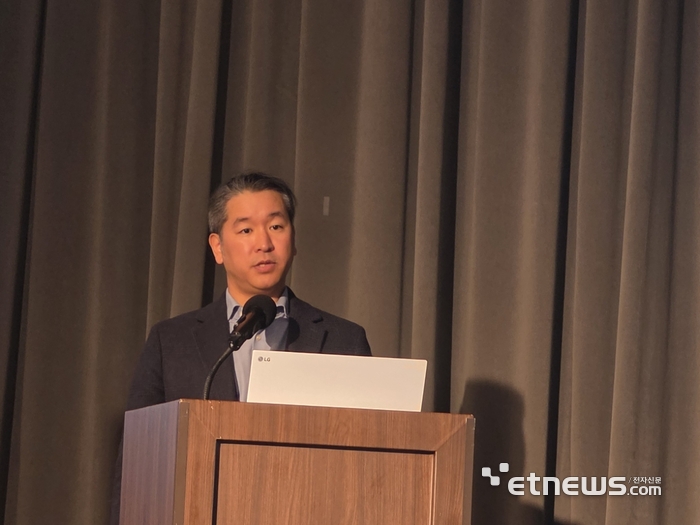
Park Ji-yong, vice president of Packaging Innovation at SK Hynix, identified the integration of heat dissipation structures within memory chips and design trade-offs as key solutions to the thermal challenges posed by increasingly tall HBM stacks.
To address localized hot spots in areas such as the physical layer (PHY) of the base die, Park said the company is “building thermal highways that remove heat by placing highly thermally conductive structures directly above those areas.”
“In doing so, we are accepting the trade-off of physically sacrificing some valuable silicon area and dedicating it to heat dissipation paths,” Park said, emphasizing that thermal management solutions have evolved to the architectural level, requiring compromises in the chip's internal design area.
Regarding the direct three-dimensional (3D) integration of HBM and logic chips, Park stressed the importance of rigorous known good die (KGD) testing, saying, “Vertical stacking worsens thermal problems, and there are harsh realities, including sharp declines in yield.”
To overcome these challenges, SK Hynix is shifting its focus toward device-technology co-optimization (DTCO) and system-technology co-optimization (STCO), which integrate everything from individual devices to entire systems.
“We have entered an era in which packaging goes beyond simply assembling chips and actually shapes the architecture itself,” Park said.
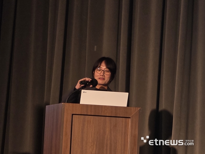
Taking the stage next, Choi Won-kyung, vice president of the Next-Generation Package Lab at Samsung Electronics' Semiconductor Research Center, expanded the discussion beyond HBM's internal architecture to the broader concept of “mega-system infrastructure,” integrating logic, co-packaged optics (CPO) and optical engines.
Choi assessed that hardware infrastructure requirements have fundamentally changed with the arrival of the agentic AI era. He also emphasized STCO as a solution to heat becoming trapped within chiplet architectures.
“Unless constraints such as heat dissipation from both the top and bottom surfaces and 3D PCD technology for controlling thermal resistance at bonding interfaces are considered from the earliest stages of die design, there is a risk of facing a major redesign at the final stage,” Choi said.
He stressed that system-level optimization must begin at the design stage.
Choi also addressed the practical realities of introducing hybrid bonding technology. He acknowledged that particle contamination control and void prevention remain extremely difficult challenges in hybrid bonding development.
To stabilize yields and costs during the initial stages of market adoption, Samsung Electronics plans to pursue a pragmatic two-track strategy, prioritizing thermocompression (TC) bonding while continuing to develop hybrid bonding. Choi said the company aims to complete mass-production validation by 2027.
Samsung Electronics also unveiled demonstration results for its 3D TCD optical engine technology, incorporating silicon photonics and CPO, as part of efforts to overcome the physical limitations of conventional copper interconnects. The company presented a vision for a total solution targeting high-speed, high-volume applications.
“We will further strengthen close collaboration with our customers and ecosystem partners to provide optimal solutions that will usher in the era of ultra-high-performance AI,” Choi said.
