

Samsung Electronics has signaled a paradigm shift in its artificial intelligence (AI) memory business model.
The company plans to move beyond the traditional memory industry's high-volume production of a limited number of products and achieve high-volume, high-mix production through collaboration with semiconductor customers to jointly design and develop memory products, responding to demand in the AI market. Innovations in the architecture and performance of AI memory, represented by high-bandwidth memory (HBM), are expected to accelerate this transformation.
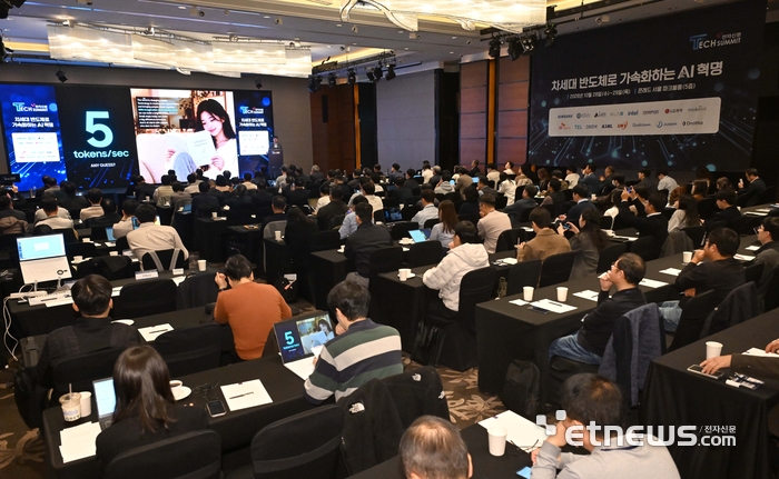
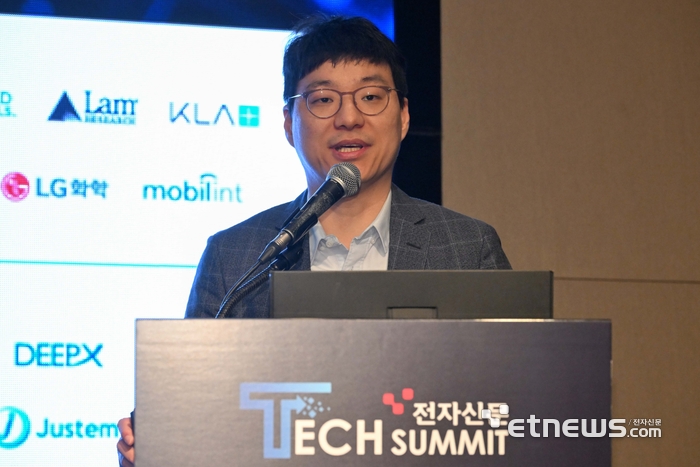
Kim Kyung-ryun, executive vice president of DRAM Development at Samsung Electronics' Device Solutions (DS) Division, emphasized the need for a new business strategy in response to changes in HBM technology and the market during a presentation titled “The Evolution of Next-Generation AI Memory” at Tech Summit 2026, hosted by The Electronic Times at the Conrad Seoul hotel on Oct. 28.
“Until now, memory has been a commodity business in which manufacturers produce identical products and sell them when orders come in,” Kim said. “HBM is currently a customized product, but in the future, it will go beyond customization to become a co-designed product.”
Conventional DRAM has been mass-produced by semiconductor manufacturers according to standardized specifications. Recently, HBM, a leading type of AI memory, has increasingly been developed to meet the specific performance requirements of individual AI semiconductor companies, including graphics processing unit (GPU) manufacturers. Kim said this approach would no longer be sufficient, arguing that it would become difficult to meet future AI requirements unless customers participate in the planning and joint design of AI memory from the outset.
“GPUs vary significantly from customer to customer, and their architectures are all different,” Kim said. “It is impossible to integrate a standardized HBM product with the AI semiconductors of multiple customers.”
Samsung Electronics is preparing zHBM to respond to this shift. zHBM is a next-generation HBM technology that improves performance and power efficiency through a three-dimensional (3D) architecture in which HBM is vertically stacked on top of a GPU. This distinguishes it from the existing 2.5D architecture, which places HBM alongside the GPU. Commercialization is expected after 2029.
Samsung Electronics expects zHBM to deliver up to eight times the performance and three times the power efficiency of HBM5, which is scheduled for release in 2028. The company also plans to improve thermal management performance by adjusting the number of stacked layers and optimizing metal layers.
“In the zHBM era, there will be a paradigm shift in both semiconductor design methods and relationships with customers,” Kim said. “Excellence in memory alone will not be enough. Comprehensive capabilities encompassing foundry services and logic semiconductors will be necessary.”
Kim assessed this as an area in which Samsung Electronics holds a competitive advantage over other memory manufacturers because the company possesses capabilities not only in memory but also in foundry manufacturing and logic chip design through its System LSI business. This is also why Samsung Electronics has recently emphasized its “total solution” approach, covering customized HBM design, contract manufacturing of customers' AI semiconductors and packaging.
“We are discussing ways to efficiently develop various types of memory in preparation for the era of high-volume, high-mix memory production,” Kim added. “We are preparing to ensure that Samsung Electronics can continue to perform well in the next-generation market.”