




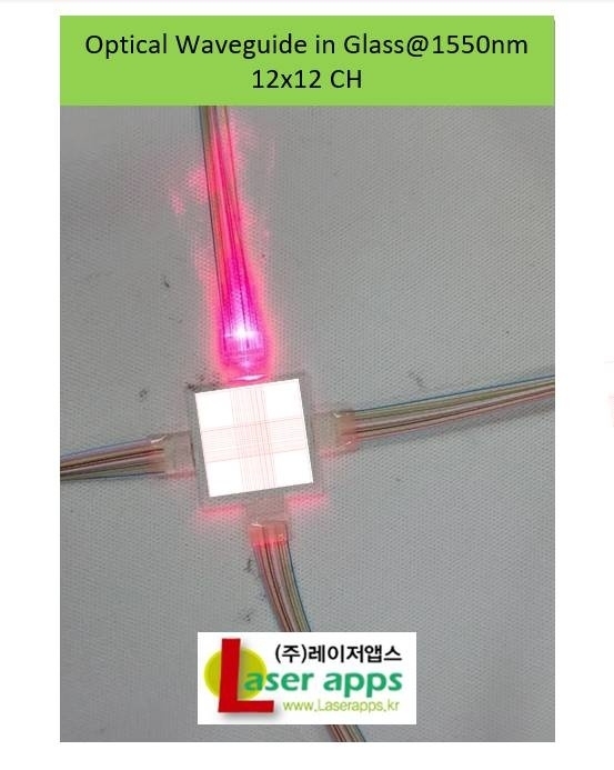
LaserApps has developed precision manufacturing technology for optical waveguides, a key component of co-packaged optics (CPO). The advance could help minimize losses as light travels through the waveguides, supporting optical interconnects designed to improve chip and system performance.
The company said it recently fabricated a waveguide for CPO with a propagation loss of 0.1 decibels per centimeter (dB/cm). The result is comparable to performance reported by leading companies in the field, marking a milestone for the South Korean small business's independently developed technology.
CPO brings optical components into the same package as semiconductor chips, enabling signals to travel as light rather than relying solely on electrical connections. Its potential to deliver faster data transmission with lower power consumption has attracted attention across the AI chip and computing industries. Nvidia and other AI chipmakers have identified CPO as a next-generation technology and are accelerating commercialization efforts.
Optical waveguides are essential to CPO. Much as electrical wiring provides a path for electrical signals, waveguides provide channels for light. Minimizing optical loss requires smooth surfaces and sidewalls, making it crucial to reduce roughness and other irregularities in the glass used to form the waveguides.
LaserApps' reported loss of 0.1 dB/cm means optical power falls by only about 2.3% for every centimeter traveled through the waveguide. In other words, most of the optical power is retained. The figure is comparable to low-loss waveguides reported by some overseas photonic integration companies, including Switzerland's LIGENTEC, the Netherlands' LioniX and companies in China.
LaserApps said its waveguides have smoother cross-sectional profiles than competing products, contributing to their quality and performance. The loss measurements were conducted in collaboration with Korea Advanced Materials.
The company fabricated the waveguides using its proprietary “plasma melting” laser technology. The process creates localized melting points inside glass and uses plasma to melt the material. According to LaserApps, this allows glass to be processed while maintaining smooth surfaces and generating virtually no microcracks.
LaserApps previously used the same technology to achieve what it described as industry-leading results in forming through-glass vias (TGVs), vertical interconnect holes in semiconductor glass substrates. Typical industry processes produce via holes 20-100 micrometers (μm) in diameter with depth-to-diameter ratios of around 5:1 to 20:1. LaserApps achieved a 72:1 ratio with a hole diameter of 15 μm.
“We have made meaningful progress with straight optical waveguides,” said LaserApps CEO Jeon Eun-sook. “We plan to continue improving performance and work toward three-dimensional optical waveguides.”
