





Samsung Electronics Co. has unveiled a next-generation three-dimensional (3D) memory architecture that vertically stacks high bandwidth memory (HBM) on top of artificial intelligence (AI) accelerators. The plan is to apply vertical chip stacking structures not only to DRAM but also to NAND flash, boosting data processing performance and power efficiency required in the AI era.
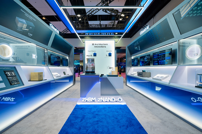
Samsung Electronics participated in FMS 2026, held at the Santa Clara Convention Center in California, US, from Aug. 4 to 6 (local time), where it unveiled mockups of its next-generation 3D memory architectures, “zHBM” and “zNAND-O,” for the first time in the industry.
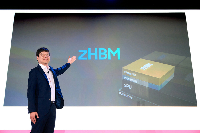
While conventional HBM is placed side by side on the same plane as AI accelerators, zHBM features a structure in which HBM is vertically stacked on top of the AI accelerator. By reducing the data travel distance between the AI accelerator and the memory, it enhances bandwidth and power efficiency.
Compared with HBM5, performance per graphics processing unit (GPU) is up to eight times higher, and performance per watt is up to three times higher. Thermal resistance was also reduced to less than half that of HBM5, mitigating heat dissipation issues occurring in stacked structures.
Another key feature is that the design can be tailored to match individual customer AI systems. Samsung Electronics added customized semiconductor intellectual property (IP) to an interlayer located between the memory and the AI accelerator, enabling memory capacity expansion or accelerator performance enhancement. The company plans to collaborate with customers to drive optimization between AI processors and memory, maximizing the performance of zHBM.
Following DRAM, Samsung Electronics also presented a 3D memory architecture for NAND flash. “zNAND-O,” currently under development, is a next-generation high-performance NAND flash solution that combines through-silicon via (TSV) technology with existing vertical stacking technology used in V-NAND. It features a structure where four-layer or eight-layer semiconductor chips are vertically stacked and packaged into a single product.
The “O” at the end of the product name signifies that it is optimized for on-device AI environments. Stacking chips vertically improves space efficiency while enhancing data loading bandwidth and response speed.
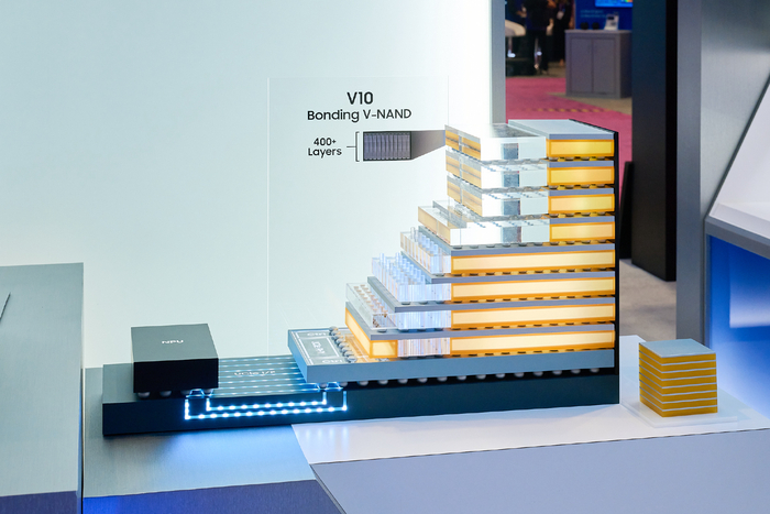
Samsung Electronics also unveiled “V10 BV-NAND,” its 10th-generation V-NAND with more than 400 vertically stacked layers, an industry first. Following its announcement of V-NAND technology at the same event 13 years ago, the company has elevated NAND technology to the next level through this ultra-high-density stacked structure of over 400 layers.
Samsung Electronics has achieved a 25% improvement in power efficiency for each generation in its V-NAND lineup. It plans to pursue energy efficiency optimization through continuous process scaling and 3D stacking technology.
Samsung Electronics also reconfirmed the HBM5 roadmap it first revealed at Computex in Taiwan in June. For HBM5, it plans to apply a base die based on a 2-nanometer (nm) process and “HPB,” a next-generation thermal management technology. HPB is a technology that adds a heat dissipation structure to the side of the HBM core die, with implementation and verification completed based on HBM4E.