








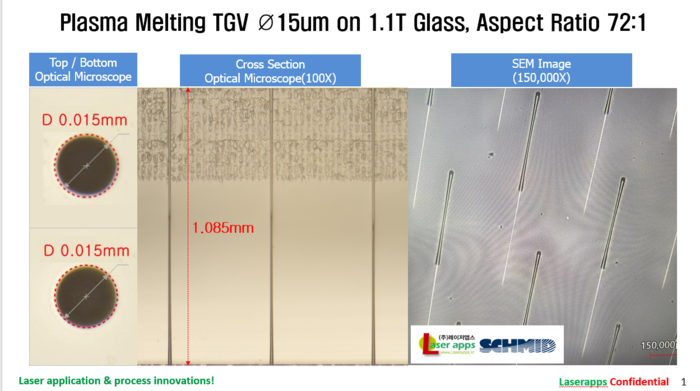
Laserapps has produced an ultra-fine, high-aspect-ratio through-glass via (TGV) sample for semiconductor glass substrates, marking a step forward in the company's effort to improve glass-core substrate performance.
TGVs are microscopic vertical passages formed through a glass substrate. Once filled with copper, they carry electrical signals between layers of a package. Smaller vias can enable higher input/output (I/O) density, helping support more advanced, higher-performance semiconductor substrates.
According to industry sources on Sep. 10, Laserapps manufactured a TGV sample with vias measuring 15 micrometers (μm) in diameter. The process was performed on glass approximately 1.1 millimeters thick, resulting in an aspect ratio of 72:1—the ratio of via depth to diameter.
The company said the vias achieved near-circular geometry and smooth interior sidewalls. A glass thickness of about 1.1 mm is suitable for glass-core substrates used as main package substrates, but it is more difficult to process than thinner glass.
TGVs are typically created by forming microscopic holes in glass using laser processing and chemical etching, then filling them with copper to establish vertical electrical interconnects. The smaller the via diameter, the more I/O connections can be integrated into the substrate.
TGV hole diameters in the industry generally range from 20 μm to 100 μm, with aspect ratios typically around 5:1 to 20:1. Laserapps' 15-μm result was achieved in relatively thick, 1.1-mm glass, making the 72:1 aspect ratio particularly notable. Existing commercial TGV offerings, for example, commonly specify via diameters beginning around 20 μm.
Laserapps had previously formed 30-μm TGVs with a 22:1 aspect ratio late last year. The latest result represents a significant advance in less than a year. The company said the work combined Laserapps' laser technology with etching technology from Germany's SCHMID.
The performance is attributed to Laserapps' proprietary “Melting TGV” technology. The method uses laser processing to create localized melt points within the glass, followed by plasma-based melting, allowing TGVs to be formed without microcracks.
“If microcracks had occurred during glass-substrate processing, we would not have been able to produce TGV holes at this level,” said Eunsuk Jeon, chief executive of Laserapps. “It once again confirms the importance of laser technology in semiconductor glass-substrate processing.”
Microcracks are a major concern in laser-based glass processing. Because high-energy laser exposure can create tiny cracks inside the glass, subsequent chemical etching may not fully eliminate them. Defects can remain or propagate along pre-existing cracks, potentially reducing substrate reliability and yield.
“Controlling microcracks is the most important challenge in securing the performance required for semiconductor glass substrates,” Jeon said.
Laserapps is supplying the TGV samples to global semiconductor glass-substrate manufacturers for evaluation. The company plans to extend the technology beyond TGV formation into other glass-substrate processes, including singulation, or precision cutting.
