








Semiconductor printed circuit board (PCB) company TLB has secured PCB process technology to mass-production levels that draws circuits with 3D printers and metallic ink. It is a digital process that draws circuit blueprints directly like printing text on paper, replacing the complex conventional photolithography process.
According to the industry on September 21, TLB succeeded in securing PCB circuit printing technology at the 50-60㎛ line width level. The 60㎛ class has reached a level capable of mass production on the line, and the 50㎛ class is at a stage where technical implementation is possible.
This is a range similar to PCBs produced through conventional process methods (roughly in the 55-60㎛ range). A width of 50㎛ is similar to the thickness of a human hair.
A PCB is a board that holds electronic components and connects electricity. The general PCB process attaches a film onto copper foil and aligns a mask. The circuit remains only after exposing it to light and developing it.
The PCB printing method skips several of these steps and directly prints the circuit. The company explains that the time to pass through the entire line (takt time) becomes shorter accordingly. TLB further shortened the time by applying a technology that attaches multiple printer heads to print a large board at once.
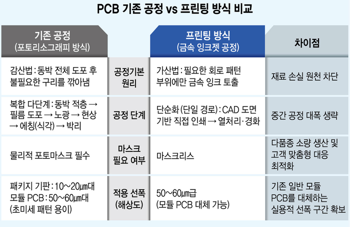
When steps are reduced, fewer intermediate equipment such as exposure machines and developing facilities need to be purchased, and the burden of chemical costs is also reduced. Because the number of times copper is melted and films are stripped decreases, the wastewater treatment burden is also smaller, making it more economical than conventional mass production lines. Since a new mask does not need to be created every time as long as the blueprint is changed, it is also advantageous for responding to customized orders from each customer.
PCB printing technology has been steadily attempted at universities and research institutes since the 2010s, but the speed of printing large-area circuits was an issue. Although a single precise circuit could be drawn, mass production—producing tens of sheets an hour like a factory—could not gain speed.
What sets TLB apart is that it secured production speed, yield, and reliability on large substrates and established a mass production system tailored to conventional factory line widths.
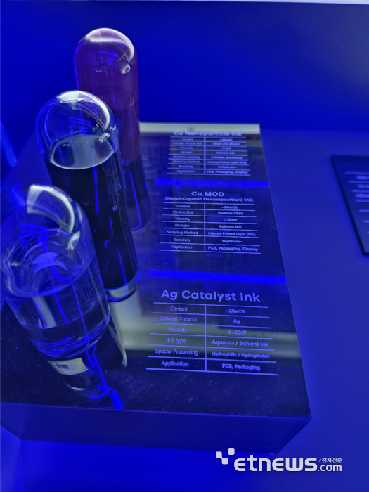
In particular, the technology secured in terms of “nano-ink” materials represents a step forward. If ink does not come out of the head, lines spread or copper does not adhere. The patented technologies secured by TLB are also focused on ink composition. Since 2021, issues such as polymer, metal ion, coupling agent, solvent ratio, viscosity, surface tension, and jetting stability have been resolved one by one. Moving the technical focus from contact pens to non-contact inkjets follows the same context.
A TLB official explained, “Because the product comes out from a single path rather than going through multiple processes, it is faster and more economical than conventional methods,” adding, “The burden of equipment unit costs, chemicals, and wastewater is reduced, making it advantageous for ESG environmental friendliness as well.”
TLB plans to coordinate the timing of commercialization after confirming order demand and going through customer verification processes.
