





Samsung Electronics says it is targeting a tenfold increase in AI response speed through zHBM, a proposed 3D-stacked memory architecture that places high-bandwidth memory directly on top of an AI accelerator.
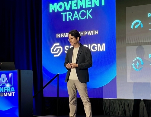
Kim In-dong, Executive Vice President for Memory Product Planning at Samsung Electronics America, outlined the company's vision on Sep. 16 at the AI Infrastructure Summit in Santa Clara, California.
“Today's conversational AI systems operate at roughly 100 tokens per second per user,” Kim said. “For agentic AI, we aim for a quantum leap to 1,000 tokens per second per user.”
Samsung argues that achieving such a jump will require moving beyond today's 2.5D packaging approach, in which high-bandwidth memory, or HBM, sits next to an AI accelerator on an interposer. The company's proposed zHBM architecture would instead stack HBM vertically on top of the accelerator, shortening the distance data must travel between compute and memory.
Kim described zHBM as the key path forward for reducing data-transfer bottlenecks in AI systems, where accelerators can spend significant time waiting for memory to supply model parameters and intermediate data.
Samsung also unveiled a roadmap for zNAND-O, a 3D NAND flash-based storage solution designed for on-device AI.
Kim said AI workstations and other local computing environments could routinely run AI models with around 1 trillion parameters by 2030, rather than relying solely on large centralized data centers.
Building enough memory for a 1-trillion-parameter model using DRAM alone would be prohibitively expensive, he said. Samsung estimates that zNAND-O could reduce the cost to roughly one-sixth of an all-DRAM configuration.
Samsung plans to begin supplying zNAND-O samples in 2028. Kim said the technology could offer customers a major advantage in time to market, which he described as a central factor in the competition to develop and deploy AI semiconductors.