








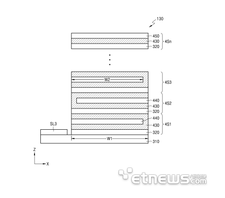
Samsung Electronics is researching a quantum computer memory structure that stacks storage components in layers rather than laying them side by side across the chip surface. The move is seen as an early bid to secure rights to a key design question, where to put memory, as quantum computers scale up to more qubits.
According to industry sources on Sep. 27, Samsung has been granted a Korean patent (KR102778201B1) for a structure that stacks superconducting qubit memory vertically instead of horizontally. Related patents from the same family (US12062826B2 and US12381298B2) have also been granted in the United States.
Unlike conventional computers, which process information as bits that are either 0 or 1, quantum computers use qubits, which can exist as a combination of 0 and 1 at the same time, a property known as superposition. Samsung's approach uses superconducting circuits, which exploit the way certain materials lose all electrical resistance at extremely low temperatures, to build qubits as circuit elements on a chip.
Conventional designs place the computing component, known as a transmon, and the component that briefly holds its results, a superconducting resonator, side by side on the chip surface. It works like a building that can only expand outward. Adding more memory means making the chip larger, which weakens the connections between components and leaves the system more vulnerable to outside noise. Qubits are notoriously fragile, and their states can be easily disrupted by temperature changes, electromagnetic noise, and vibration.
Samsung's patent addresses this by stacking the memory vertically. A thin superconducting waveguide layer containing the resonator sits on the substrate, topped by an insulating layer that blocks electrical current and then a superconducting shielding layer that blocks noise. This three-layer structure repeats multiple times. The waveguide and shielding layers are each about 50 to 100 nanometers thick, while the insulating layer is about 200 to 600 nanometers thick. The shielding layers in odd- and even-numbered stacks face opposite directions.
The design offers three main advantages: more memory fits into the same footprint, the layers sit close enough together to couple efficiently, and the top shielding layer blocks outside electromagnetic waves, reducing signal disruption.
The approach also plays to Samsung's core strengths. The company has long increased capacity by stacking NAND flash vertically and layering high-bandwidth memory (HBM). Building up superconducting films, insulating layers, and shielding layers one on top of another is essentially an extension of those chip-stacking processes.
Samsung Advanced Institute of Technology (SAIT) has also been working on scalable quantum processors that pair superconducting multi-qubit chips with control chips designed to operate at cryogenic temperatures. The new patent can be seen as one answer from that research effort to the question of how to integrate memory.
“This research is less about building a finished quantum computer and more of an early-stage effort to test how uniformly and densely superconducting qubits can be fabricated using semiconductor processes,” an industry source said.
