








Samsung Electronics has filed a groundbreaking patent aimed at resolving critical reliability bottlenecks in High Bandwidth Memory (HBM) packaging. As the industry approaches the ultra-high-stack era of HBM4E and HBM5, Samsung is fundamentally redesigning the “dummy die”--the protective top layer of the memory stack--to dramatically improve structural stability and manufacturing yields.
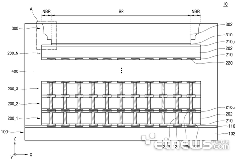
According to patent documentation disclosed on June 28, Samsung has developed a sophisticated technique that shapes the outer edges of the topmost dummy die into a three-tiered, stepped, contoured structure. This geometric innovation is specifically engineered to mitigate delamination, micro-cracking, and warpage (wafer warping), which have become persistent failure modes in high-stack architectures.
Traditional HBM architectures consist of multiple core memory dies vertically stacked on top of a base die, with a non-electrical dummy die placed at the very top. This dummy die ensures the total package conforms to strict standard height specifications while providing physical protection and thermal dissipation.
However, as stacks aggressively transition from 12 layers to 16 layers and beyond, the reliability of this top layer has emerged as a major variable for fab production yields and long-term device stability. Historically, upgrading from an 8-layer to a 12-layer stack triggers a 10 to 20 percentage point drop in yield. Moving toward 16 layers causes yields to fall even further into the 40% to 60% range. Optimizing the structural design of the dummy die directly addresses this issue by neutralizing warpage and managing coefficient of thermal expansion (CTE) mismatches.
To implement this structure, Samsung utilizes a high-precision “deep groove sawing” process. Unlike conventional mechanical blade dicing, this advanced technique carves ultra-precise, deep channels into the wafer before die separation. By leveraging laser technology, it minimizes structural damage to the semiconductor's crystalline matrix.
The resulting layout forms an inverted-pyramid silhouette, in which the bottom bonding surface of the dummy top die remains narrow while the upper surface expands outward. The side profile features distinct primary, secondary, and tertiary facets characterized by discontinuous gradient shifts and upwardly convex curves. This unique contour delivers substantially higher mechanical strength than conventional vertical-cut sidewalls.
Furthermore, Samsung has pre-fabricated micro-trenches within the Non-Bonding Region (NBR). This structural addition effectively traps microscopic dicing debris generated during the sawing phase, preventing contamination of critical bonding interfaces and bolstering the overall reliability of the fusion-bonding process.
Thermal management has also been heavily optimized. The patent specifies a tightly controlled vertical distance of 1 to 10 micrometers between the lower face of the bonding insulation layer and its horizontal extension, maintaining ideal heat-dissipation efficiency. It also introduces a modified protruding surface profile that minimizes the required volume of the epoxy molding compound (EMC), opening up a more direct thermal path for heat escape.
Samsung is expected to integrate this structural advancement with its current suite of advanced HBM packaging technologies, such as hybrid bonding and Heat Path Blocks (HPB). By enhancing holistic package reliability, the company aims to aggressively expand its footprint in the highly competitive global HBM market.
Industry insiders note that in high-stack configurations of 12 layers and above, top-die warpage is a make-or-break variable impacting final production yields. Experts view this newly unveiled patent as a forward-looking foundation explicitly targeted at perfecting yield dynamics for 16-layer HBM5 nodes.
