








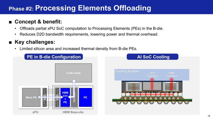
Samsung Electronics and SK hynix laid out sharply different approaches to easing next-generation high-bandwidth memory, or HBM, bottlenecks at Hot Chips 2026, with Samsung focusing on making the HBM base die more intelligent and SK hynix emphasizing advanced packaging and thermal management.
The two companies presented their strategies during the Memory Technology tutorial on the opening day of Hot Chips 2026 at Stanford University on Aug. 23 local time. Samsung's Sangwook Han presented “HBM Base Die: How HBM Will Evolve Using Advanced Logic Processes,” while SK hynix's Jaesik Lee presented “Advanced Packaging for High Bandwidth Memory.”
Samsung is pursuing what it calls the activation of the base die, transforming the bottom layer of an HBM stack from a relatively simple interconnect component into an active logic chip. SK hynix, meanwhile, is focusing on advanced packaging technologies that address heat dissipation and warpage as HBM stacks add more layers.
HBM consists of DRAM core dies, or C-dies, stacked above a base die. Samsung said it is shifting the base die from a conventional DRAM manufacturing process to a 4-nanometer-class logic process beginning with HBM4 and HBM4E. The move is intended to improve power efficiency and create room for additional functions within the base die.
In the first stage of its roadmap, Samsung plans to replace the conventional physical-layer interface with an advanced-logic-based die-to-die interface, reducing area requirements and moving the memory controller into the base die. It also plans to add an SRAM-based repair function capable of repairing defects across multiple dies.
To address heat, Samsung introduced a Heat Path Block, or HPB, which it said can cut peak temperature by more than 35%.
The second stage would add system-on-chip-level reliability functions, including temperature, voltage and aging sensors, as well as on-chip self-test blocks. Samsung also presented the concept of “advanced HBM,” incorporating an external-memory direct-connect interface and processing elements capable of handling data preprocessing tasks.
In the third stage, known as zHBM, Samsung proposes eliminating the interposer and vertically stacking the compute chip directly with DRAM stacks. Using wafer-on-wafer bonding and hybrid copper bonding would shorten input-output paths and substantially reduce power consumption.
Samsung said the base die could evolve from a simple interconnect layer into a coprocessor, reshaping how memory and logic are designed for AI systems. The company has said zHBM could deliver 70% greater power efficiency and 230% higher DRAM bandwidth than a conventional HBM4E stack.
SK hynix focused on packaging technology for HBM stacks of 16 layers or more. HBM uses through-silicon vias, or TSVs, to connect stacked core dies to the base die in a three-dimensional architecture. As stacking density and bandwidth rise, thermal resistance and warpage become increasingly difficult challenges.
SK hynix said its mass-reflow molded underfill, or MR-MUF, technology—already in mass production—improves warpage control and enables finer pitches and narrower gap filling. The company said it has reduced package height to 775 micrometers, cut chip thickness to 90% of the previous level and lowered gap height by half.
For the next generation, SK hynix highlighted hybrid bonding. The technology could allow core dies to be made 24% thicker, reduce TSV pitch to below 18 micrometers and lower thermal resistance by 35% even as stack heights increase, according to the company.
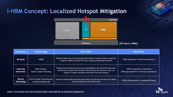
Lee also discussed SK hynix's iHBM technology, formally introduced in May. iHBM places a highly thermally conductive but electrically insulating cooling material in the die-to-die physical-layer area, where heat is concentrated, to create a dedicated heat path. The localized hotspot-management approach is similar in purpose to Samsung's HPB and is expected to reduce thermal resistance by roughly another 30%.
“Over the longer term, we plan to pursue three-dimensional integration that stacks HBM directly on top of accelerators,” Lee said. “For HBM4, we are targeting more than a 14% improvement in thermal resistance, over 40% better power efficiency, bandwidth above 2 terabytes per second and capacity of up to 48 GB, compared with HBM3E.”
