





Major Chinese semiconductor equipment companies are accelerating the localization of back-end packaging equipment, leveraging the technology they established in front-end manufacturing.
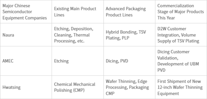
According to industry sources on the 5th, Chinese semiconductor equipment firms such as Naura Technology Group, Advanced Micro-Fabrication Equipment (AMEC), and Hwatsing Technology are expanding the application of their existing front-end technologies—including etching, deposition, and chemical mechanical polishing (CMP)—into back-end packaging tools tailored for hybrid bonding, dicing, and wafer thinning.
This expansion is viewed as a strategy by China to broaden its equipment self-reliance into advanced packaging amid U.S. chip export controls. In particular, as the boundaries between front-end and back-end processes blur due to the growth of High Bandwidth Memory (HBM) and 3D stacking, the room to adapt and extend existing front-end technologies into back-end equipment has grown significantly.
China's largest equipment maker, Naura, recently stated in its half-year report that it launched two types of 12-inch hybrid bonding equipment—wafer-to-wafer (WTW) and die-to-wafer (DTW)—and that the DTW tool has entered the customer integration stage.
Hybrid bonding is a technology that precisely joins chips and wafers to stack multiple chips densely, such as in HBM and chiplets.
This year, Naura also released process equipment dedicated to Through-Silicon Via (TSV) electroplating and Panel-Level Packaging (PLP). By offering tools that fill micro-vias with copper to connect chips vertically, as well as equipment for line formation and surface treatment on large panels, the company has expanded its footprint in advanced packaging.
AMEC, a leading Chinese etching equipment vendor, is expanding its reach from existing TSV etching to dicing and deposition. Its plasma dicing tool, which separates wafers into individual dies, advanced to the validation phase at major domestic customers this year.
In the first half of the year, AMEC also initiated the development of deposition equipment for Under Bump Metallization (UBM), a tool that forms metal layers beneath chip interconnections.
AMEC set a goal to cover more than 70% of the equipment portfolio required for advanced packaging over the next five years through in-house R&D and mergers and acquisitions (M&A). The plan is to broaden its packaging tool portfolio beyond TSV etching to encompass dicing and deposition.
Hwatsing, whose core business is CMP equipment, is also extending its technical scope to advanced packaging. After supplying select advanced CMP tools to the HBM production lines of major Chinese memory manufacturers, Hwatsing added dedicated packaging equipment lines, including wafer grinding and edge processing. In the first half of this year, it shipped its new 12-inch wafer grinding equipment for advanced memory for the first time.
“Faced with U.S. export controls that restrict advanced node scaling, China is pursuing a strategy to offset individual chip performance limits through advanced packaging,” said Oh Jong-hyuk, researcher at Korea Institute for International Economic Policy (KIEP). “As interconnecting multiple chips to boost total computing capacity becomes vital, the scope of equipment localization is naturally expanding into back-end processes.”
However, many of the new tools disclosed by Chinese vendors remain in customer validation or early commercialization stages. Whether these companies can prove yield rates, equipment operational stability, and productivity in actual mass-production lines will likely determine their future market expansion.