




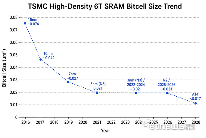
TSMC plans to shrink its high-density 6T SRAM (static random-access memory) bit cell to below 0.017 square micrometers (μm²) on its A14 process, which is targeted for volume production in 2028. That would end a stall in SRAM scaling that began with the N5 (5nm) node in 2020, when the cell size settled at 0.021 μm².
According to industry sources on Oct. 26, TSMC will present research results later this year showing that it has achieved the world's smallest SRAM cell, below 0.017 μm², along with best-in-class SRAM macro density. Based on publicly available figures, that would give A14 the smallest cell size among TSMC, Intel and Samsung Electronics.
Intel's most recent disclosure for its 18A process came at last year's ISSCC. It reported a high-density cell of 0.021 μm² and a macro density of up to 38.1 megabits per square millimeter. Some comparisons put 18A's block density on par with TSMC's 2nm, but its cell area is still larger than A14's. Samsung adopted gate-all-around (GAA) transistors relatively early. But it has published few specific SRAM cell figures for its latest processes, which makes a direct comparison difficult.
SRAM is the ultra-fast cache memory built into CPUs, GPUs and AI accelerators. The smaller the bit cell, the basic unit of memory, the more memory fits in the same area, which directly affects performance and power efficiency. As process nodes advanced, however, SRAM proved hard to shrink because of structural limits. Many analysts have noted that TSMC's high-density 6T SRAM bit cell has barely shrunk since N5, including at N3 and N2.
Discussion of chip scaling usually centers on logic circuits. As feature sizes shrink, more transistors fit in the same area, which boosts computing performance and cuts power consumption. SRAM, by contrast, serves as on-chip scratch storage. It has to keep its contents stable while data is being read and written, and that requirement makes it harder to scale.
As a result, SRAM cells stayed large even as feature sizes shrank, and SRAM took up a growing share of chip area. That share is a particular problem for chips like AI accelerators, which have to move large volumes of data quickly. When the cache is too small, the chip has to make frequent trips to external memory, so overall performance falls short of expectations even if raw compute speed improves. A smaller SRAM cell means chipmakers can now scale down storage as well as compute.
TSMC says A14 is aiming for 10-15% faster speed, 25-30% lower power consumption and roughly 20% higher chip density than N2, its previous generation. The company attributes the density gain to both logic and SRAM scaling.
Memory bottlenecks are becoming a bigger problem for AI and high-performance computing chips. If SRAM density improves again, designers can fit a larger cache in the same die area, or the same cache capacity in a smaller footprint. However, several factors remain undisclosed, including yield at volume production, cost, customer adoption and whether A14 will use backside power delivery (BSPDN).
TSMC said it has also developed technologies for system-level integration. These include an innovative redistribution layer that supports a 4.5 μm SoIC (3D stacking) bond pitch, high-performance capacitors and through-silicon vias. “Backed by good yields and device progress, A14 technology is on track for volume production in 2028,” the company said.
