








Samsung Electronics has objectively demonstrated the technical advantages of its high-stack packaging strategy for next-generation High Bandwidth Memory (HBM4E).
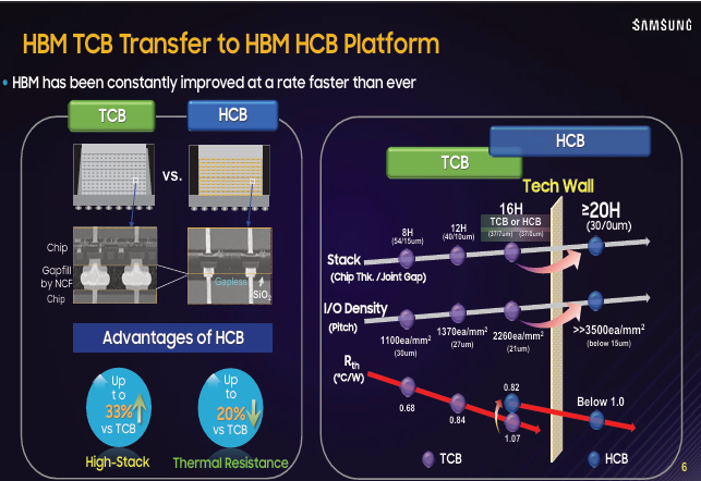
The company has published the industry's first quantitative study showing that Hybrid Copper Bonding (HCB) offers significantly superior thermal management compared with the conventional Thermo-Compression Bonding (TCB) process.
According to industry sources on June 25, Samsung researchers systematically validated HCB's thermal advantages over TCB through multi-scale modeling and experiments using actual test chips under server-class operating conditions. Going beyond conventional chip- and package-level simulations, the study demonstrates HCB's superiority in realistic high-stack environments.
The findings underscore Samsung's differentiated packaging strategy relative to TCB and Mass Reflow-Molded Underfill (MR-MUF) technologies, highlighting advantages not only in electrical performance but also in thermal management and long-term reliability.
The technology is expected to become particularly important for future HBM4E products with 16 or more memory layers, where heat dissipation becomes increasingly challenging. The study, titled System-Level Thermal Analysis of Hybrid Cu Bonded HBM for 2.5D Advanced Packaging, was published this month by the Institute of Electrical and Electronics Engineers (IEEE).
Samsung developed a physics-based multi-scale numerical modeling framework capable of analyzing thermal behavior from microscopic chip structures to package- and server-level systems. The model incorporates metal interconnects and dielectric thin-film effects at the chip level before extracting effective thermal properties for package- and system-level simulations.
To validate the model, the researchers mounted HCB- and TCB-based HBM test vehicles alongside ASIC test chips on a silicon interposer and conducted measurements under air-cooled conditions representative of real server environments.
The experiments showed that HCB produced lower hotspot junction temperatures than TCB, reducing the risk of overheating. Thermal interference between the HBM stack and the underlying ASIC was also reduced, minimizing heat transfer between the memory and logic chips. Under identical cooling conditions, HCB allowed for higher power budgets, providing greater headroom for performance improvements.
In addition, HCB reduced stack height by more than 15%, resulting in a thinner package that further improved thermal dissipation.
Unlike TCB, which relies on micro-bumps and underfill materials that interrupt heat transfer paths and increase thermal resistance, HCB uses direct copper-to-copper bonding, creating more efficient heat conduction pathways. Samsung also conducted a parameter study on HCB bonding pad density, proposing design optimizations that could further enhance thermal performance.
Samsung's research team said the predictive design framework developed through this study will be used to evaluate bonding technologies and optimize thermal performance in next-generation high-performance computing (HPC) packaging architectures.
