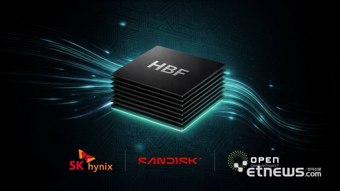






SK Hynix announced on August 4 that, together with SanDisk, it unveiled the first standard specifications for High Bandwidth Flash (HBF), a next-generation storage technology based on NAND flash memory.
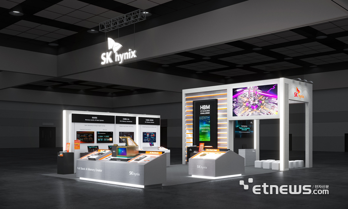
SK Hynix stated on August 4 that it presented the specifications while participating in 'FMS (Future of Memory and Storage) 2026,' the world's largest memory conference held from August 4 to 6 (local time) at the Santa Clara Convention Center in California, U.S.
HBF is a new memory technology developed to hold more data than High Bandwidth Memory (HBM) while processing data faster than Solid State Drives (SSDs). Like HBM, which stacks multiple layers of DRAM, HBF stacks NAND flash vertically to increase capacity and data transfer speed. It is considered a next-generation technology to reduce memory bottlenecks in situations where data volume pours out due to artificial intelligence (AI) inference.
These specifications are the first result released about six months after SK Hynix launched a consortium in February this year, following its collaboration on HBF standardization with SanDisk in August last year.
The capacity was defined up to a maximum of 512GB based on two stack configurations that stack NAND dies in 8 layers and 16 layers. The bandwidth was divided into three tiers to support from 0.4 terabytes (TB) to 3.0TB per second.
As the connection method linking HBF and processors, the industry standard UCIe was adopted. This established a foundation to flexibly connect and use HBF with different types of processors, such as Graphics Processing Units (GPUs) and Central Processing Units (CPUs).
The specifications were disclosed through the Open Compute Project (OCP), the world's largest open data center technology collaboration organization, so that the entire industry can utilize them.
Google and AI semiconductor company Tenstorrent are currently participating in the HBF Consortium. SK Hynix plans to expand participating companies to increase technology maturity and market acceptance, accelerating the establishment of the HBF ecosystem.
SK Hynix will also reveal for the first time at this event the 10th-generation (V10) 375-layer 4D NAND wafer and products under development. Early next year, it plans to begin mass production of high-performance, high-capacity enterprise SSDs (eSSDs) applying this technology.
“As AI adoption spreads rapidly, it is a point where redesigning the entire data processing structure is required,” said Cheonseong Kim, head of solution development at SK Hynix. “Through HBF, we will expand the boundary between memory and storage and contribute to implementing a new architecture that improves overall system efficiency.”